Automatic Test Equipment (ATE)

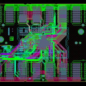
Layers and Traces: Different colors represent different layers of the PCB, where each layer can contain traces (wires) or other features like vias (vertical connections between layers). The traces are paths that connect various components on the PCB.
Components: The dark gray regions likely represent component footprints where different electronic parts like resistors, capacitors, or integrated circuits (ICs) are placed and soldered.
Routing: The colorful lines represent the routing of electrical connections between components. This routing is crucial for the functionality of the PCB, ensuring that signals and power are properly distributed.
Pads and Vias: The small circles and larger blocks represent pads and vias. Pads are where component leads are soldered, and vias are used to connect traces from one layer to another.
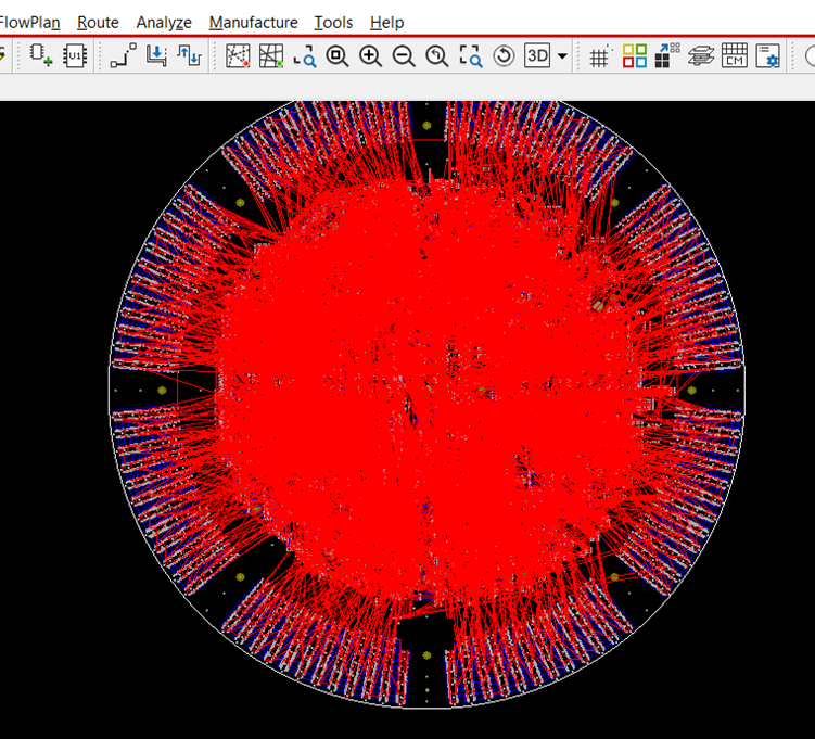
Dense Routing: The Blue lines represent a high density of electrical connections, suggesting a complex design. This is common in PCBs for advanced electronics, where many connections are needed in a compact space.
Component Placement: The central area likely houses the main components, with connections radiating outward to other components around the perimeter.
Multilayer Design: The different colors and dense network indicate a multilayer PCB, where multiple layers of conductive material are stacked to allow for more complex circuit designs.
Software Interface: The presence of the software interface at the top suggests that this design is being viewed and edited in a PCB design tool, such as Altium Designer, Eagle, or KiCad. These tools allow engineers to create and simulate PCB layouts before manufacturing.


Schematic Design: Engineers start by creating a schematic diagram, which is a logical representation of the electronic circuit.
Component Placement: Components are placed on the PCB layout in a way that optimizes space and electrical performance.
Routing: Electrical connections (traces) are routed between components. This step is crucial for signal integrity and performance.
Verification: The design is checked for errors, such as unconnected pins or overlapping traces.
Manufacturing: The finalized design is sent to a manufacturer, where the PCB is fabricated and assembled with the components.

Our design team having more than fifteen years of experience in all Major ATE test platform and commercial projects.
- Load boards (LB),
- Handler Interface Board (HIB),
- DUT Interface Board (DIB)
- Universal probe cards,
- Probe cards (Vertical/Cantilever), Spider cards, Probe Interface Board (PIB), Flexible PCBs
- Device Characterization Boards,
- Burn in Boards.
- Reference Design & Development,
- Reverse engineer
Tester Types
- Verigy
- Eagle
- Teradyne
- LTX/Credence
- Advantest
- chroma tester
- etc…


Board Design Skills
- Controlled Impedance/Delay matching.
- High speed designs involving Serdes.DDR4 & DDR5
- Blind and Buried via and Mechanical visa’s
- Expertise in high speed digital, RF and mixed signal.
- Copper coin process for high temperature.
- High speed backplane.
- Precision analog and mixed signal integration.
- RF and microwave design skills.
- Adherence to IPC/MIL standards.
- Design of low power consuming boards using power management techniques.
- ROHS compliance design.
Board Design Experience
- All designs are schematic driven and layouting applies signal integrity rules.
- Differential pairs
- Adherence to IPC Standards – IPC-2221, IPC-2222, IPC-2223, IPC-7351 etc.
- Skew matching as per the signal rise time
- Optimal board stack up with ups with controlled impedance for micro stripline,stripline and dual stripline stackups
- Faster manual routing with in-house tools avoiding vias with good aesthetics
- Designed boards with blind and buried vias, Micro-via and via-less routing, constraint driven placement and routing

Leave A Comment